How does a photodiode detectors works
The electromagnetic radiation that hits the substance could be absorbed, reflected, or even traverse the material with only a slight reduction of its intensity. The detectors for electromagnetic radiation are designed to ensure that the largest portion of the radiation that is incidentally absorbed is absorbed into them.

The optical radiation forms part of the vast electromagnetic spectrum that covers the wavelength range of 10 nm up to 100 um. This spectrum is divided into 3 sub-bands
- ultraviolet radiation (l<380 nm)
Visible radiation (l =380 - 780nm)
Infrared radio (l>780 nm)
The optical radiation of corpuscular wave nature, which means that it could be viewed as a propagating wave with frequency U or as the result of a stream of photons each one carrying energy.
Wf=hu
where h is Planck's constant. Since there is a relationship between the length and frequency of a wave
l =c/u
in which c is the speed of light, the wavelength corresponding to the energy of a photon is determined by the relation:
l f = hc/ Wf
The phenomena of electrical energy that arise in the presence of radiation are often referred to as photoelectric phenomena. They may be both internal and external. The phenomenon of external photoelectricity occurs when the intensity of the photons is enough that electrons excited by optical light escape from the body's surface which is why photoemission happens. When the power of photons is lower, meaning that there is no possibility of photoemission however, there is a slight alteration in the energy level of the body's electrons the phenomenon of photoelectricity is known as internal. The photoelectric effect can be seen as increased electrical conductivity for a semiconductor, or dielectric material, in which it is known as the photoconductor phenomena, or through the development the electromotive force within an element with an p-n junction clearly defined and in this case, it is known as the photovoltaic phenomenon.
Photodetectors that utilize the photoelectric effect from outside (photocells or photomultipliers) are currently used in special equipment, e.g. for precise measurements using photometry. Today, the most commonly used photodetectors utilize the photoelectric effect inside. This includes photodiodes, photoresistors as well as phototransistors and phototristors. If you want to know how does a photodiode work check the hyperlink. You should know theory behind this diode before reading.
The fundamental photoelectric phenomena in semiconductors results in the formation in free charge carrier resulting from an absorption process of electromagnetic radiation. There are two fundamental mechanisms:
Interband that leads into the release electrons and a hole
Doping which leads in the release electrons or hole.
The process of interband absorption is when the photon's energy Wf=hu exceeds the bandwidth that is forbidden by the semiconductor, as well as the dopant absorption mechanism is activated is when the energy Wf is less than Wg is more than Wj, the amount of energy generated by the ionization of dopants within the material. Thus, the long-wavelength threshold for radiation absorption, which is characterized by the broadest wavelength of radiation absorption from the material (recorded in the detector).
l max=hc/Wg lub l max=hc/Wj
Also, there exists a minimal range of wavelengths of radiation that are detected in the detector. This is due to the increasing absorption coefficient a p when the radiation's wavelength diminishes. As a result of which the radiation regardless of the rise in photon energy, causes weaker and weaker production of carriers. This is because, in the absence of a way to penetrate into the substrate the material, it is absorbed by the thin and thinner surface layer.

The rise in the number of free charge carriers caused by illumination of a semiconductor by radiation at the right wavelength is manifested as an improvement in the electrical conductivity. This extra conductivity is known as photoconductivity, as opposed to the dark conductivity caused by the thermal excitation of carriers. Photoconductivity only occurs in a particular portion of the radiation spectrum that is different for every semiconductor material.
In the photoconductivity phenomenon it is important to note that there exist positive as well as negative charge carriers (dual-carrier mechanism of current conduction) is crucial. This allows for massive amounts of charge carriers, and at the same time preserve the resultant neutrality of electrical energy not just in the overall system however, it can also be maintained locally (it is worth noting this that photoconductivity doesn't not occur in the realm of metals where there is only one kind charged carriers).
In such detectors there are always physical processes involved: the production of charge carriers through electromagnetic radiation that strikes the semiconductor and transportation (transport) of the carriers across the semiconductor region to contacts of the metal that connect this semiconductor to an outside electrical circuit and finally the interaction of the photocurrent that flows into the contacts and the electrical circuits of the outside. The exact nature of the mentioned processes typically differs in the various types of semiconductor detectors. It is what determines the efficiency of these devices and the potential of their use.
It is common to hear the expression "spectral sensitivity" or "relative spectral sensitivity". This is a reference to the voltage or current sensitivities that characterize the detector for a specific wavelength of radiation. Typically, the spectral sensitivity is expressed by the graph S(l) . In the context of relative spectral sensitivity, in this instance, we mean as sensitivity that is proportional to its highest value:
S(l)/Smax(l).

Vacuum photoelements
Photoelectrodes made of vacuum (photocells) are constructed by an atomized diode that is an extremely thin layer of material with a visible photoeffect is placed to the outside of a glass bulb from inside and forms the cathode. The anode is positioned in the middle of an oblong ring made of wire in order to block as much as possible the cathode which radiation of light passes. Quantities of light with sufficiently high intensity (hv > the amount of work required for electrons leaving the metal) generate photoelectrons. They, in turn, when they reach the positively polarized apex of the anode result in a flow of current within an external circuit. The strength of the present is proportional both the intensity of light that is reflected off the photocathode as well as the wavelength of light. Photocathodes are typically constructed from a mix of silver, cesium oxide and pure cesium. the photo effect is evident at a distance of 1.1um.
Photocathodes that are filled with noble gas (argon) at lower pressure are also found. Photoelectrons ripped from the cathode result in the gas to ionize filling the photocell. This leads to an increase of energy (5 or 12 times).
The main drawbacks of vacuum photoelectrodes are the high voltage of supply exceeding hundreds of volts as well as the inability to miniaturize.
Photomultipliers
Photomultipliers are vacuum photoelements where they, in addition to the photocathode, there's an array of electrodes that are covered by a material that has an excellent coefficient in secondary electron emissions. The electrodes (dynodes) are polarized using a an increasing potential that is gradually increasing, the variation in voltage between electrodes of this kind is around 100 V. Electrons that are knocked out of the photocathode, and accelerated due to the voltage difference between the cathode as well as the first electrode to hit its surface, cause knock-out of secondary electrons the quantity of which is more than the amount of electrons. Secondary electrons that accelerate in the electric field that is created between the first dynode to the following one trigger another emission of electrons onto its surface. This is the process repeats on the surface of any subsequent positive polarized electrodes. When the amount of electrons ejected on the surfaces of the successive dynodes increases, we observe the phenomenon of duplicates of the initial quantity of photoelectrons knocked from the photocathode's surface. In the end, the electron stream arrives at the anode that is at the maximum potential. The advantage of photomultipliers lies in their extremely sensitive, they permit the measurement of single quantums of light! (If we consider that the coefficient of emission of secondary electrons emanating from on the surface of the Dynode to be equal to 10, and the number of duplicating electrodes is 8 and we will get a duplication of more than 108 times ).
The negatives of photomultipliers are the need for supplying the highest voltage, which can range from 1500 V. Then there is the absence of miniaturization and inability to resist vibration and shock.
Photoresistors
A photoresistor is referred to as a junctionless semiconductor component which, when subjected to the effects of light radiation drastically alters its resistance. The active (light-sensitive) portion of the photoresistor is made up of a thin semiconductor layer that is deposited onto the dielectric substrate, along with metal electrodes which supply electricity from any external source. The entire thing is put in an enclosure that has a window to transmit light. A light beam with the correct wavelength causes the formation of electron-hole pairs. This increase in the number of electrons and holes improves that conductivity in the semiconductor leading to a reduction in resistance to the photoresistor.

Current-voltage characteristics of the photoresistorfor different values of illumination intensity.
The most popular photoresistors may be constructed from these materials, including lead sulfur (PbS) as well as led teluride (PbTe) in either its intrinsic or activated in a suitable way (Ge) and indium antimony (InSb) and Cadmium sulfur (CdS).
The properties of light-resistance are represented by the relationship between this photoresist's resistivity RE upon the intensity of illumination E. This can be approximately described by an equation that is empirical:
In this case, Ro is the resistance of the photoresistor at level of the Eo (usually 10 lx) and it is a constant variable and the amount of which is largely dependent on the type that semiconductor materials are made of (for CdS, g =0.5-1).
When it comes to the use of photoresistors for radiation detectors the following aspects of technology are paramount significance:
Temperature of the detector T - by detector temperature, is the temperature of the active area, and for photoresistors , the temperature the semiconductor layer which is subject to light has during detector operation.
The Active area in the detector for photoresistors, this can be said that it's what is the surface of the semiconductor which is illuminated.
The electrical parameters that relate with the operation point of the photoresistor, the permissible voltage between ends of the photoresistor's Umax , the maximum electrical power dissipated from the photoresistor Pmax, the resistance's dark voltage at a particular voltage at its ends and the voltage that determines its operating points.
The sensitivity of the detector - each detector operates within a certain range in which the magnitude that the signal output is proportional the signal input. In this range, the ratio between these two values is known as"detectors sensitivity. For radiation detectors, the current sensitivities or voltage sensitivity are listed.
The term "current sensitivity" refers to proportion of increase of the photoelectric short-circuit current to the flux of radiation incident in the detector.
The term "voltage sensitivity" refers to the proportion of the increases of the photoelectric voltage at the resistance of the load (when it is matched) to the flux of radiation that is reflected off the detector.
Sensitivity units for radiation detectors are amperes for Watt or volts per watt or volts per watt, for example .
Time constant of the detector is the time constant of signal increase and fall; the amount of time needed to achieve 1-e-1 of the maximum value of the signal (about 63 percent). Time constant for decay of signal (also known as the time needed for a signal to diminish to e-1 of its highest value (about 37 percent ).
In the description abbreviated of the photoresistor rather than the RE(E) property, instead of the RE(E) characteristic we will use the value of the resistance to dark (i.e. the amount of resistance that the photoresistor experiences when its area of the active is totally dark) as well as the brightness resistance RE, for a particular amount of brightness E (most typically E = 1000 lx) are typically listed. The most important parameters specific to photoresistors are still the maximum voltage that is permissible, Umax which is the maximum amount of energy that the element can dissipate and the temperature sensitivity coefficient that is average.
Semiconductor photodiodes
Photoelectric instruments that have barriers, also known as known as semiconductor photodiodes are generally Pn junctions in which the dispersion of the concentration of minor carriers occurs by the force of photons that reach this junction via a window that is built into the photodiode's housing. Photodiodes' pn junctions are constructed from a variety of semiconductors, the most popular ones being germanium (Ge) as well as silicon (Si) along with gallium arsenide (GaAs) and Cadmium thermoplastic (CdTe). Within the barrier layer on the junction two kinds of phenomena can occur as a result of the illumination. An electromotive force develops (photovoltaic photovoltage phenomena) and the voltage passing through the junction increases with the intensity of the photon as the junction becomes turned towards the opposite direction (photodiode).
A photodiode is activated only when it is reversed in the negative direction. If the state is dim (in light absence light) just the darkness current is flowing through the photodiode. This corresponds to the reverse voltage that flows through the junction, determined by thermal production of carriers. The light source at the junction is responsible for the creation of additional carriers and an increase of the reverse current of the junction, dependent on the amount of radiation that is reflected.
Photodiodes feature their high operating speeds (much greater than phototransistors or photoresistors) that can reach several hundred MHz. In cases where speeds are required specific photodiode designs are employed: pin photodiodes and avalanche photosiodes.
In a pin-type photodiode the intrinsic semiconductor that is sandwiched within doped regions p,n. In this kind of structure the barrier layer has an enormous thickness, roughly similar to that of the inner layer which results in the capacitance of junctions extremely small as well as the lower inertia for photodiode operation.
A avalanche photodiode can be described as an element that operates within the breakdown range of avalanche in the Pn junction.
If a minority-carrier such as an electron that is generating the phenomenon of a saturation current, gets increased in the field that is electric in the junction to the kinetic energy of or more than 3/2 Eg the electron could transfer a portion the energy it has to an electron in the valence band, and then ionize it to the conduction band. This creates an electron-hole pairing and the electron decreases its energy of kinetic. We now have two electrons and one hole which are able to acquire energy through the electric field of the junction between the pn and the. When they achieve energy levels of 3/2 Eg each could generate a new electron-hole pair. The process repeats itself several times in an avalanche-like fashion. Avalanche breakouts are usually found within a variety of areas known as "microplasmas ". Microplasmas act in a sporadic manner and conducts current that is multiple pulses. Avalanche breakthrough takes forms of random bursts the sum of which creates massive noise across a large frequency range. Within the range that is avalanche breakout it is proportional to voltage of the power that is between 3,6. Iw is the reverse of that current. Iw can be expressed by an equation that is empirical:
Iw=MIo
where Io is the saturation current , M is the multiplication factor.
In the event of an multiplication by avalanche of the number of carriers created by light that is produced, the rise in current due to the illumination on the diode will be greater than M which is M, the multiplication factor that is dependent on the voltage at which the photodiode is polarized. Avalanche photodiodes typically have designs specifically designed to detect visible radiation that is modulated by a high-frequency sound, and also rapidly growing pulses of the radiation.
Photocell
If there is a multiplication caused by an avalanche of the number of carriers produced by light and the current that is increased caused by the light that is reflected off the diode is greater than M, which is M, the multiplier factor which is dependent upon what voltage the diode is in polarization. Avalanche photodiodes are typically equipped with design that is specifically designed to detect visible light that is modulated with the high frequency sound. It also has the ability to detect rapid increasing pulses of radiation.
Phototransistors
Phototransistors, also known as bipolar transistors (usually the npn type) where a window is created in the housing to permit illumination of the transistor's base. Phototransistors are polarized as a normal transistor. i.e. that the emitter base junction gets located in the direction of conduction, and the collector junction at the base is negatively polarized. Typically, phototransistors are constructed in two-terminal form, i.e. the collector and emitter contacts are made visible, and the base area is left unconnected. In the absence of light there is no current flowing through the phototransistor. This is in connection with the generation of thermal carriers. This is the current flowing through the negatively polarized pn junction that lies at the edge of the collector and base areas.
The illumination of the base region with radiation of the appropriate wavelength leads to the appearance of negative and positive electron carriers, electrons and holes within the phototransistor's base because of an the internal photo-effect. The inexplicably polarized base-collector junction results in the separation between carriers (analogous to the process that occurs in a photodiode that is too polarized). Minority carriers that are under their influence by the electrical field that is present at the interface between base and collector can be "flipped" to the collector. A majority of them are accumulated in the base region, which reduces the potential barrier at the junction between emitter and base, which allows for majority carriers to travel through the emitter area and into that of the base. The carriers that are in the base area are considered minority carriers. the extreme polarization of the junction between collector and base allows them to move to the collector zone and also increases the current of collectors.
The characteristics of the output Ic=f(UCe) are similar to the characteristics of bipolar transistors. The value doesn't refer to base current instead, it is the intensity of the region of base. The most commonly used type of phototransistors used is npn.
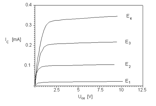
Family of phototransistor output characteristics for different illumination values.


No comments: